A circuit board with numerous layers of conductive material is known as a multilayer PCB. An insulating substance is utilised to sandwich and bind these layers, forming a substrate that can support electronic components. The Multilayer PCBs, which are the most prevalent kind, have at least three layers of conductive material. PCBs with high-density interconnect (HDI): These PCBs are frequently utilised in high-frequency and high-speed applications because they have a higher component density than conventional multilayer PCBs. These PCBs are utilised in applications where the PCB needs to be bent or flexed and are made of flexible materials like polyimide. These PCBs combine the advantages of flexible and conventional multilayer PCBs. This article discusses in depth overview of Multilayer PCB.
A multilayer PCB (printed circuit board) is a circuit board that has multiple layers of conductive material. These layers are sandwiched together and bonded with insulating material, creating a substrate that can be used to support electronic components.
Multilayer PCB is commonly used in a variety of electronic devices, such as computers, smartphones, and other types of consumer electronics. They are also used in industrial, military, and aerospace applications.
The multiple layers of conductive material in a multilayer PCB allow for more complex and flexible circuit designs, as well as increased component density and improved signal integrity. They also provide added support for components, increasing the overall reliability of the PCB. In addition, the increased component density and improved signal routing of multilayer PCBs allow for smaller and lighter PCBs to be designed.
Multilayer printed circuit boards have grown in popularity recently across a variety of industries. One of the causes of increasing popularity is the rise in demand for small gadgets. Users may actualize denser designs with multilayer PCBs without sacrificing performance. Multilayer PCBs are widely used in many of the common items we use, from tiny wearables to vital communications equipment.
Do you want to know the applications for multilayer PCBs? The top six uses for multilayer PCBs Fabrication are covered in this article.
The medical sector depends heavily on electronic equipment. The medical sector is embracing downsizing just like any other sector that depends on electronics. The demand for tiny gadgets in the medical sector has expanded as non-invasive treatment methods gain popularity.
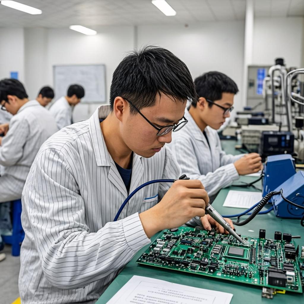
Consumer electronics, sometimes known as home electronics, refers to a broad range of electronic devices made for regular use. This typically includes technology for entertainment (smart TVs, music players, etc.), communication (smartphones, laptops, etc.), and kitchen appliances (microwaves, washing machines, etc.)
Industrial electronics are very different from consumer electronics in many ways. They are subjected to unfavorable conditions such high temperatures, shock, vibrations, pressure, dust, and humidity.
Today, it is difficult for us to envisage a world without automation and computers. Multilayer PCBs are used in everything, including computers and associated devices like graphics cards, motherboards, computer mice, and more, due to their space-saving and functional qualities. Compared to other competing technologies, these PCBs can be developed to deliver higher performance at lower costs.
Similar to the aforementioned sectors, numerous militaries and defense applications are beginning to priorities multilayer PCBs. These PCBs are high-speed electronics that are favored for their small size, light weight, usefulness, and durability.
Many telecommunications devices, including GPS and satellite applications, signal transmission, and other applications that call for longevity while keeping a high level of performance, use multilayer PCBs. Increasing-performance, sophisticated tiny devices are in high demand due to the advent of wireless technology.
Multilayer printed circuit boards (PCBs) come in a variety of designs and serve a variety of functions in electronic systems and gadgets.
These multilayer PCBs are the most prevalent kind, and a variety of electronic systems and gadgets use them. They can have anywhere between 4 and 20 layers and are made up of numerous layers of laminated conductive and non-conductive materials.
These multilayer PCBs, which have a lot of connections in a tiny space, are frequently employed in systems that need a lot of downsizing. They can utilize microvias and other approaches to enhance the number of connections, and they can have more layers.
These flexible multilayer PCBs may be stretched and curved to fit into various shapes and places since they are constructed of flexible materials like polyimide. They are frequently utilised in gadgets like wearables and smartphones that need a lot of flexibility.
These multilayer PCBs combine the advantages of flexible and stiff PCBs. They can be employed in applications that call for both stiff and flexible PCBs since they have a combination of rigid and flexible layers.
These are multilayer PCBs that employ vertical connections between layers known as buried or blind vias to enhance the number of connections while minimizing PCB size. They are frequently employed in high-speed and high-density applications.
A multilayer PCB includes at least three or more conductive layers, and through-hole, blind, or buried vias are used to make the electrical connection between these conductive layers. The demand for complicated PCBs has greatly expanded as a result of the advancement of technology in the electronics industry. A few benefits of multilayer PCBs are their small size, increased robustness, high assembly density, low weight, etc. Due to these benefits, they are the finest option for practically all electronic applications, including consumer electronics, telecom, automotive, medical equipment, satellite communication, and many more.
Many features found on ceramic multilayer PCBs are absent from conventional circuit boards. It is superior to all other printed circuit boards because of these benefits. The benefits listed do not apply to a particular type of ceramic PCB. Instead, these are the common benefits that are present in the majority of multilayer circuit boards with ceramic bases. Among the benefits are.