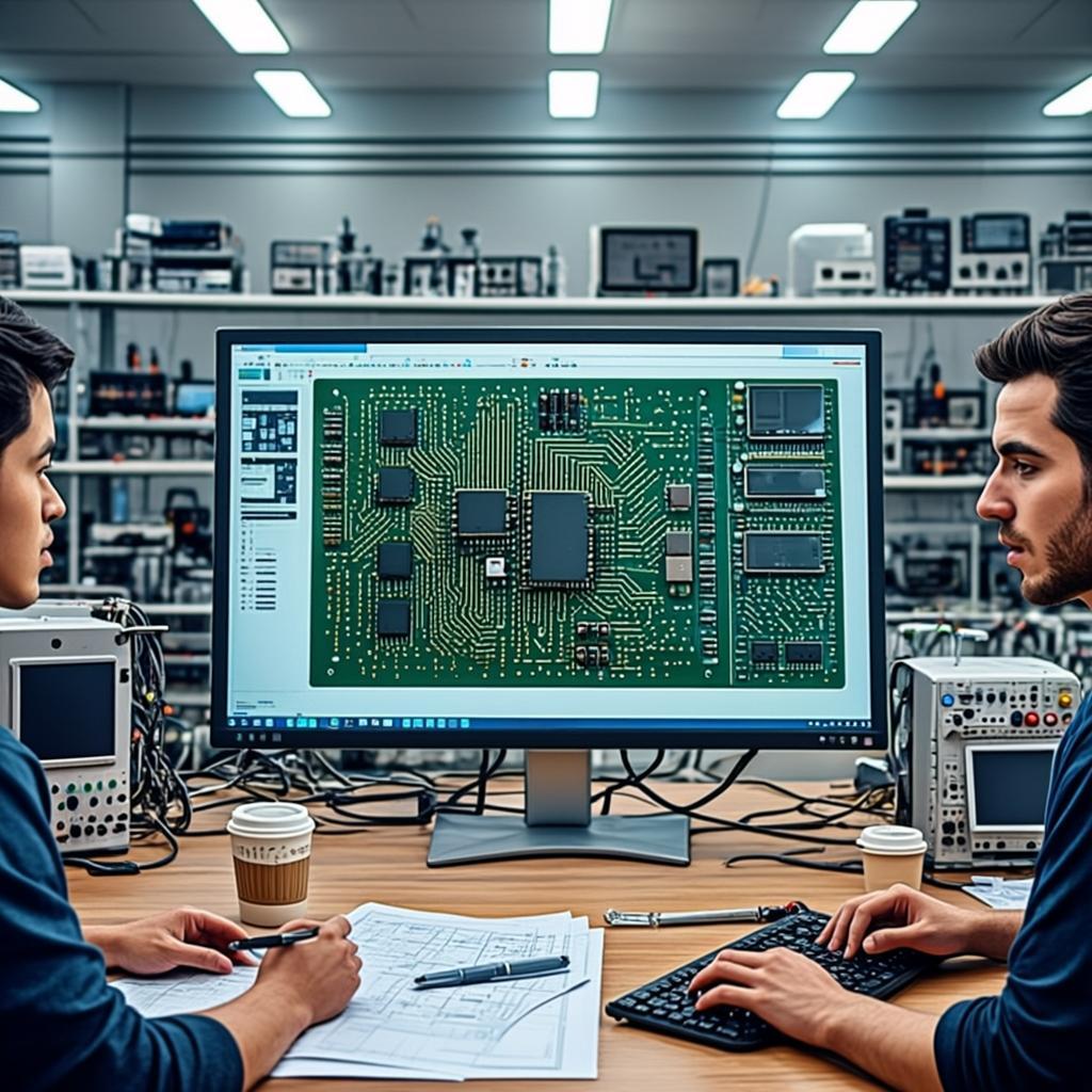
Thanks to these features, it is possible to efficiently connect even very complicated components such as Ball Grid Arrays (BGAs) or system-on-chip modules in a minimal space. Here, conventional printed circuit boards quickly reach their physical limits – HDI offers the solution.
It is anything but trivial to build an HDI circuit board. Unlike standard PCBs, sequential lamination is often used for high-density interconnect boards. This means that the layers of the circuit board are built up and connected to each other one after the other, like a multi-story building with precisely planned connecting tunnels.
A key term in this context is "ELIC" – Every Layer Interconnect. This design integrates continuous microvia interconnects in all layers, enabling highly flexible connections. Even so-called Type III structures, based on IPC-2226 (Sectional Design Standard for High Density Interconnect Printed Boards), which combine multiple micro-via and buried-via layers, are widely used, especially in complex multi-layer designs with high pin density.
Shorter distances result in faster signals and fewer disruptions.
Microvias can be used to distribute heat in a targeted manner.
Thanks to compact structures, it is possible to completely redesign products.
Although HDI technology is advantageous, it also presents certain challenges. It brings new challenges, particularly in design and manufacturing. Laser drilling, multiple laminations, precise registration accuracy and microfine structures require specialized manufacturing processes.
The costs are also considerable: the production of HDI boards is more expensive than that of conventional multilayer PCBs – both in terms of the materials used and the manufacturing equipment and quality control required.
HDI-PCBs are not just an option – they are the answer to the pressure for innovation in compact high-performance systems.
HDI technology is often the engine of modern electronics. Without these circuit boards, autonomous vehicle systems, smartwatches, or portable diagnostic devices would be unthinkable. It enables powerful high-frequency electronics to be housed in the smallest of spaces – with high reliability and energy efficiency.