Printed Circuit Board Assembly (PCBA) plays a pivotal role in the world of electronics manufacturing. Think of PCBA as the essential step that brings a PCB to life, making it ready for use in everything from consumer gadgets to complex medical equipment.
In this article, we'll break down PCBA—its definition, types, processes, and quality control—giving you a clear understanding of how important it is in today's electronics industry.
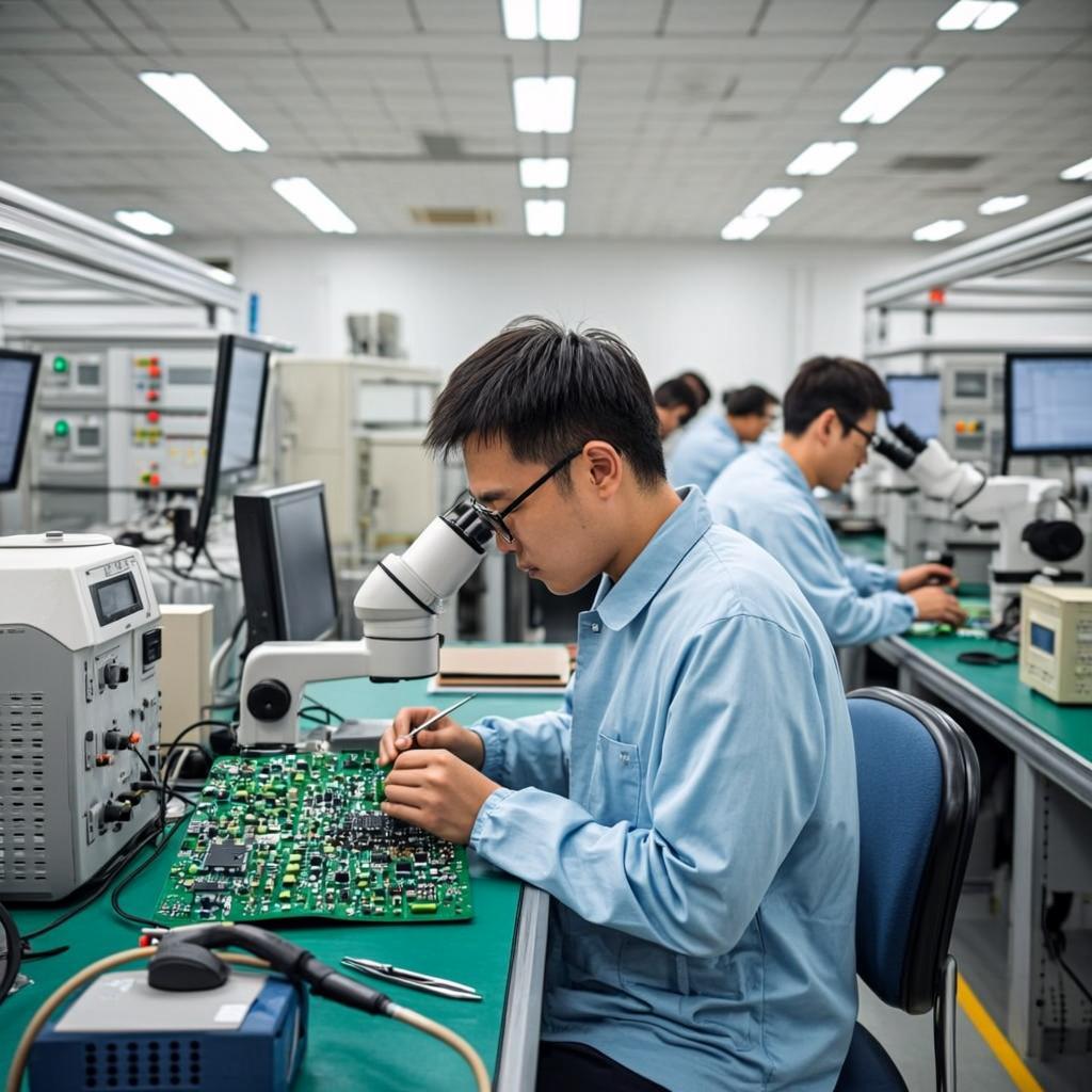
Printed Circuit Board Assembly (PCBA) refers to the process of mounting and soldering electronic components onto a printed circuit board (PCB) to create a functional electronic assembly.
A PCBA not only includes the bare board itself but also all the resistors, capacitors, connectors, and integrated circuits that deliver the final device's functionality.
PCB Assembly is the broader term for the end-to-end activities required to transform a bare PCB into a working electronic module.
This process encompasses stencil printing of solder paste, placement of surface-mount and through-hole components, reflow or wave soldering, and post-solder inspections.
In industry parlance, "PCBA"and "PCB assembly"are often used interchangeably, but PCBA focuses on the result—the assembled board—PCB assembly covers each step in the production line, including design for manufacturability (DFM), pick-and-place programming, and final functional testing.
When comparing a bare PCB to a fully assembled PCBA, the distinction is clear:
The roots of PCBA trace back to the 1950s, when early electronic circuits were hand-wired point-to-point. The invention of the printed circuit board in 1956 revolutionized electronics by etching conductive pathways on insulating substrates.
In the 1960s and 1970s, through-hole technology (THT) became standard for mounting bulky components. The 1980s saw the introduction of Surface Mount Technology (SMT), which allowed for higher component density and automated pick-and-place machines.
Over the past four decades, continual innovations in reflow soldering, automated optical inspection (AOI), and design-for-manufacturability (DFM) software have driven PCBA toward ever-smaller, more reliable, and cost-effective assemblies—paving the way for today's compact smartphones, wearables, and Internet of Things devices.
To help you quickly compare the main PCBA methods and decide which best fits your project needs, here is an at-a-glance overview:
In addition to the core SMT, THT, and hybrid methods, modern electronics often leverage specialized assembly approaches to meet unique space, performance, or reliability requirements:
Ultra-small solder ball arrays enable very high pin-count ICs to be mounted in compact footprints. Common in smartphones and high-speed computing modules.
Boards are stacked or folded to create three-dimensional structures, maximizing functionality in constrained volumes—ideal for wearables and compact IoT devices.
Bare silicon dies are directly bonded and wire-bonded onto the PCB, then encapsulated. This technique reduces component height and improves signal integrity.
BGA packages sit on a grid of solder balls, providing excellent thermal performance and electrical connectivity for high-pin-count devices used in servers and advanced controllers.
Each of these advanced techniques fills a specific niche—highlighting the importance of selecting the right assembly method to balance size, performance, cost, and reliability in your final product.
By following a series of standardized PCB assembly steps—from solder-paste printing to final inspection—manufacturers ensure reliable electrical connections, optimal performance, and consistent product quality.
Understanding this end-to-end workflow is essential for design engineers, procurement specialists, and anyone sourcing PCB assembly services.
1. Design for Manufacturability (DFM) Review
Engineers validate the PCB layout against manufacturing constraints (clearances, pad sizes, thermal reliefs).
2. Solder Paste Application
A steel stencil deposits a uniform layer of solder paste onto each copper pad.
3. Pick-and-Place
High-speed machines accurately position surface-mount devices (SMDs) onto the pasted pads.
4. Reflow Soldering
The board passes through a controlled-temperature reflow oven, melting solder and forming permanent joints.
5. Through-Hole Insertion & Wave/Selective Soldering
For through-hole components, leads are inserted and soldered via a wave or selective process.
6. Cleaning & Flux Removal
Any residual flux is cleaned—often with aqueous or solvent methods—to prevent corrosion.
7. Inspection & Testing
Automated Optical Inspection (AOI), X-ray, In-Circuit Test (ICT), and Functional Test verify solder integrity and circuit functionality.
PCBA is the bridge between bare-board fabrication and finished electronic products. By integrating component mounting, soldering, and testing into a streamlined production line, PCB assembly enables high volume, consistent quality, and fast time-to-market. Key advantages include:
CAD software sits at the heart of the PCB assembly process, offering tools for schematic capture, layout editing, and DFM rule checking. Modern PCB CAD platforms generate pick-and-place data, stencil artwork, and Gerber files that drive every downstream assembly step.
By catching layout errors early and automating data export for stencil printers and pick-and-place machines, CAD integration slashes lead times and reduces miscommunication between design and manufacturing teams.
By leveraging automated pick-and-place machines and reflow soldering ovens, PCBA delivers placement accuracy down to ±0.01 mm and repeatable solder joint quality.
This level of automation minimizes human error, increases throughput (often exceeding 20,000 CPH—components per hour), and ensures consistent alignment of fine-pitch components.
Modern PCBA lines use lead-free solders (e.g., SAC305 alloy) and closed-loop solvent systems, reducing hazardous waste by over 60% compared to legacy processes.
Water-jet or ultrasonic cleaning recycles 80% of rinse water, supporting RoHS and WEEE compliance while lowering disposal costs.
1. Rapid Prototyping: Integrated stencil and pick-and-place data from CAD allow first-article builds within 24–48 hours.
2. Concurrent Processes: DFM review, stencil setup, and placement programming run in parallel to fabrication.
3. Streamlined Supply Chain: Vendor-managed inventory (VMI) for components reduces lead times by up to 40%.
Effective PCBA testing is critical to guarantee product reliability, reduce field failures, and comply with industry standards.
By integrating testing at multiple stages, manufacturers can detect assembly defects—such as solder bridges, opens, and misalignments—before boards leave the factory. This not only minimizes costly recalls but also strengthens customer trust in your brand.
Design for Manufacturability (DFM) directly impacts how effectively a board can be tested. Early DFM reviews identify problematic footprints, inaccessible test points, and tight spacing that hinder fixture design or probe access.
By prioritizing testability during the layout phase, you can:
Effective quality assurance (QA) in PCB assembly combines inline process controls with post-assembly inspections to catch defects early and maintain consistent yield.
Key QA methods include Solder Paste Inspection (SPI) to verify paste volume, Automated Optical Inspection (AOI) for component placement and solder-joint quality, In-Circuit Test (ICT) for electrical connectivity, and Functional Test for end-use performance.
By integrating these checks into the PCB assembly line, manufacturers reduce rework rates and ensure each board meets stringent reliability criteria.