High Frequency and High Speed PCB by Application (Computer Field, Communication Field, Automotive Field, Consumer Electronics, Others), by Types (Double Board, Multilayer Board), by North America (United States, Canada, Mexico), by South America (Brazil, Argentina, Rest of South America), by Europe (United Kingdom, Germany, France, Italy, Spain, Russia, Benelux, Nordics, Rest of Europe), by Middle East & Africa (Turkey, Israel, GCC, North Africa, South Africa, Rest of Middle East & Africa), by Asia Pacific (China, India, Japan, South Korea, ASEAN, Oceania, Rest of Asia Pacific) Forecast 2026-2034
The High Frequency and High Speed PCB market is poised for substantial expansion, projected to reach an estimated USD 15,000 million by 2025, with a robust Compound Annual Growth Rate (CAGR) of 12.5% through 2033. This impressive trajectory is fundamentally driven by the insatiable demand for advanced electronic components across a multitude of burgeoning sectors. The proliferation of 5G infrastructure, the rapid advancement of autonomous driving technologies, and the ever-increasing complexity of consumer electronics are all pivotal forces propelling this growth. As devices demand faster data transmission and lower signal loss, high-frequency and high-speed PCBs become indispensable, enabling the intricate circuitry required for these cutting-edge applications. The communication field, in particular, is a major consumer, as network infrastructure, advanced smartphones, and high-speed data centers rely heavily on these specialized boards. Furthermore, the automotive industry's transition towards electrified and connected vehicles, incorporating sophisticated sensor arrays and high-bandwidth infotainment systems, adds significant momentum to market adoption.
The market's dynamism is further shaped by several key trends and restraints. Innovations in materials science, leading to the development of novel dielectric materials with improved electrical properties, are a significant trend, facilitating higher performance and reliability. The miniaturization of electronic devices, coupled with the need for enhanced thermal management, also fuels the demand for more sophisticated PCB designs. However, challenges such as the high cost of specialized materials and manufacturing processes, alongside stringent quality control requirements, present considerable restraints. Geographically, the Asia Pacific region, led by China, is expected to dominate the market due to its extensive manufacturing capabilities and the presence of numerous key players in the electronics supply chain. While North America and Europe are also significant markets, driven by innovation in their respective automotive and telecommunications sectors, the sheer volume of production in Asia Pacific is likely to maintain its leading position. The competitive landscape is characterized by the presence of established global players, all vying for market share through continuous product innovation and strategic collaborations.
The High Frequency (HF) and High Speed (HS) Printed Circuit Board (PCB) sector is characterized by a strong concentration of innovation and expertise among a select group of global manufacturers. These companies are heavily invested in advanced materials, sophisticated manufacturing processes, and rigorous testing methodologies to meet the demanding requirements of modern electronic systems. Key characteristics of this sector include the need for extremely tight impedance control, low signal loss, and exceptional thermal management. Innovation is driven by the relentless pursuit of higher data rates and lower latency, pushing the boundaries of material science and fabrication techniques.
While direct regulatory impact on PCB manufacturing is often indirect, stringent Electromagnetic Interference (EMI) and Electromagnetic Compatibility (EMC) standards globally influence material selection and board design. Product substitutes are limited, with specialized HF/HS PCB materials being largely irreplaceable for high-performance applications. End-user concentration is significant, with the computer and communication fields being the primary drivers of demand. The level of Mergers & Acquisitions (M&A) within this niche segment is moderate, as companies focus on consolidating expertise and expanding technological capabilities rather than broad market acquisition. The market size for HF/HS PCBs is estimated to exceed $7,500 million globally in the current year, with significant portions attributable to advanced computer and communication infrastructure.
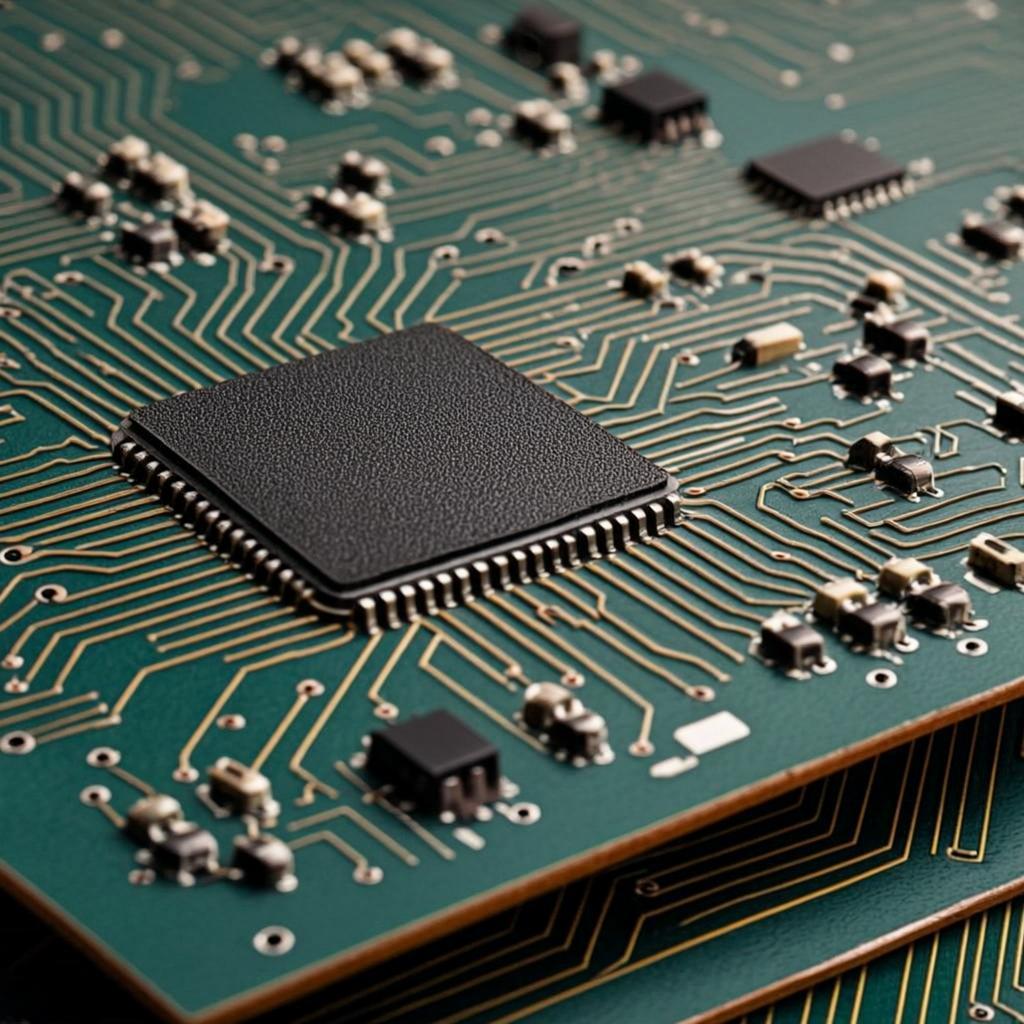
High Frequency and High Speed PCBs are designed to handle signals operating at gigahertz frequencies and data rates exceeding 10 Gbps. This necessitates the use of specialized low-loss dielectric materials, such as PTFE composites and advanced epoxies, to minimize signal attenuation and distortion. Precision in trace width, spacing, and dielectric thickness is paramount for achieving controlled impedance, typically within a 1% tolerance. Advanced fabrication techniques, including blind and buried vias, sequential lamination, and complex multilayer stacking, are employed to maximize interconnect density and minimize signal path lengths, thereby reducing latency and crosstalk. The integrity of these boards is crucial for the reliable operation of cutting-edge applications in telecommunications, high-performance computing, and advanced radar systems.
This report provides a comprehensive analysis of the High Frequency and High Speed PCB market, segmenting it across key application areas, product types, and regional landscapes.
The global High Frequency and High Speed PCB market exhibits distinct regional dynamics. North America leads in demand driven by its robust telecommunications infrastructure build-out (5G) and a strong presence of technology giants in the computer and defense sectors. Asia-Pacific, particularly China, is the manufacturing powerhouse, with a vast ecosystem of suppliers and a rapidly growing domestic market for communications and consumer electronics. Europe shows steady growth, fueled by automotive advancements and a focus on industrial automation and telecommunications upgrades. Emerging markets in other regions are gradually increasing their adoption as digital transformation accelerates.
The High Frequency and High Speed PCB landscape is undergoing rapid evolution, driven by the insatiable demand for faster data rates and lower latency. A dominant trend is the increasing adoption of advanced dielectric materials beyond standard FR-4, such as specialized PTFE (Polytetrafluoroethylene) composites, modified epoxies, and hydrocarbon-based laminates. These materials offer significantly lower dielectric loss tangents (Df) and lower dielectric constants (Dk), crucial for signal integrity at frequencies exceeding 10 GHz. The industry is witnessing a surge in demand for boards supporting 5G and future 6G wireless communication infrastructure, necessitating PCBs capable of operating reliably at millimeter-wave frequencies.
Furthermore, the complexity of HDI (High-Density Interconnect) technology is escalating, with an increased reliance on techniques like laser drilling, microvias, and back-drilling to minimize signal reflections and improve routing efficiency. Thermal management has become a critical design consideration, as higher power densities in advanced processors and RF components generate substantial heat. This is leading to the integration of thermal vias, metal-core PCBs, and specialized thermal management materials. The miniaturization trend continues, pushing for smaller form factors without compromising performance, which drives the development of advanced multilayer PCBs with intricate stacking and fine-line features. The automotive sector's increasing sophistication in ADAS and autonomous driving is another significant trend, requiring robust, high-reliability HF/HS PCBs that can withstand harsh environmental conditions. The development of next-generation data centers and AI/ML applications also fuels the demand for high-performance computing PCBs with superior signal integrity and power delivery. The global HF/HS PCB market size is projected to surpass $9,000 million by 2028, with these trends contributing significantly to its growth.
The High Frequency and High Speed PCB market is propelled by several powerful forces:
Despite strong growth drivers, the High Frequency and High Speed PCB sector faces notable challenges: