At the heart of every modern electronic device lies its printed circuit board (PCB). More than just a platform for components, the PCB is the central nervous system of your product, determining its performance, reliability, and longevity. The choice of your PCB manufacturer is therefore not a simple procurement step; it is a strategic engineering decision.
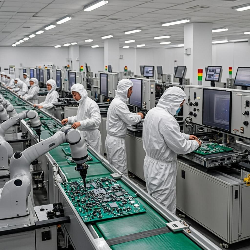
A design file is a perfect, theoretical model. Transforming it into a high-functioning physical board is where professional manufacturing makes the critical difference. This process hinges on several key capabilities:
Signal Integrity & Material Science: High-speed digital and high-frequency RF designs (like those in 5G and IoT devices) demand precise control over electrical signals. Professional manufacturers achieve this through expertise in selecting specialized materials (like Rogers or Isola laminates) and controlling impedance with tolerances as tight as ±10%. Amateur fabrication can lead to signal loss, crosstalk, and data corruption.
Power Integrity & Thermal Management: Modern processors and ASICs require stable, clean power. This is ensured through sophisticated multilayer stack-ups with dedicated power and ground planes. Furthermore, effective thermal management via thermal vias and appropriate copper weights (e.g., 2oz for power circuits) prevents overheating, ensuring device stability and a longer lifespan.
Miniaturization and Reliability (HDI): As devices shrink and become more powerful, High-Density Interconnect (HDI) technology is essential. This involves advanced processes like laser-drilled micro-vias (as small as 0.1mm), stacked vias, and fine-line etching (3/3 mil line/space). These techniques allow for more functionality in a smaller footprint, which is critical for wearables, medical implants, and advanced consumer electronics.
In non-critical applications, a PCB failure might mean an inconvenience. However, in several advanced industries, the stakes are significantly higher:
Automotive: PCBs must withstand extreme temperatures, constant vibration, and humidity. They are the backbone of safety systems like ABS and airbag control units. Failure is not an option.
Medical: Devices for diagnostics and patient monitoring require absolute reliability. They often need to be biocompatible and manufactured in certified cleanrooms to ISO 13485 standards.
Aerospace & Defense: Boards must perform flawlessly under intense stress and in harsh environments, adhering to stringent standards like IPC-A-610 Class 3.
Choosing EBest Circuit (Best Technology) means partnering with experts who translate your complex designs into reliable, high-performance hardware. We bring over 19 years of focused expertise in advanced PCB and flexible circuit manufacturing. Ready to discuss how our manufacturing capabilities can bring robustness and reliability to your next project? Contact our engineering team at pcb@frankenthalerfoundation.org for a consultation.
Selecting the appropriate PCB type is a foundational engineering decision that directly impacts the performance, reliability, and cost of an electronic device. Moving beyond basic definitions, a deeper understanding of the classifications and their manufacturing implications is crucial. Here is a detailed breakdown based on industry standards and advanced fabrication capabilities.
This is the primary way to categorize PCBs, reflecting their complexity.
Single-Sided PCBs: Featuring a single conductive copper layer on one side of a substrate, these are the most straightforward to manufacture. They are cost-effective and ideal for simple, low-density circuits but offer limited functionality for modern devices.
Double-Sided PCBs: These boards have conductive layers on both the top and bottom surfaces, connected by Plated Through-Holes (PTH). This doubles the available area for components and routing, making them a versatile and common choice for a wide range of applications, from industrial controls to consumer electronics.
Multilayer PCBs: Defined as having three or more conductive layers, these boards are essential for complex, high-speed electronics. Layers are laminated together with insulating prepreg (PP) under high temperature and pressure. Capability Spotlight: Modern manufacturing, as detailed in your materials, can produce boards with up to 32 layers. High-TG (Glass Transition Temperature) materials, such as KB6167 or IT180, are often mandatory for boards exceeding 8 layers to ensure stability during the lamination process and under operational heat.
The base material defines the physical form of the board, enabling innovative product designs.
Rigid PCBs: The most common type, built on inflexible substrates like FR-4. They provide excellent mechanical support and are used in the vast majority of electronic equipment where the board does not need to move or bend.
Flexible PCBs (FPC): Manufactured on flexible plastic substrates like polyimide. Their key advantages include high flexibility, light weight, and excellent resistance to heat and vibration. They are perfect for dynamic applications or tight spaces, such as in cameras, wearable devices, and within automotive assemblies.
Rigid-Flex PCBs: This advanced hybrid integrates rigid boards for component support with flexible interconnects into a single structure. This combination simplifies the overall assembly, enhances reliability by eliminating the need for connectors between rigid boards, and allows for more compact, three-dimensional packaging.
The surface finish is a critical quality factor, protecting the copper from oxidation and ensuring solderability. Your document lists an extensive portfolio, including:
HASL (Hot Air Solder Leveling): A common, cost-effective finish for general purposes.
ENIG (Electroless Nickel Immersion Gold): Provides a flat surface, excellent for fine-pitch components and offering good oxidation resistance.
Immersion Silver/Tin: Offers good performance for a range of applications.
ENEPIG (Electroless Nickel Electroless Palladium Immersion Gold): A premium finish with superior wire-bonding capability and resistance to corrosion.
Gold Finger Plating: Used for edge connectors, requiring a hard, durable gold plating. Combinations like HASL + Gold Finger or ENIG + OSP are also standard offerings to meet specific zone-specific requirements on a single board.
For high-performance applications, the base laminate material is specially engineered.
High-Frequency/High-Speed PCBs: These use specialized laminates (e.g., Rogers, Taconic) with controlled dielectric constants (Dk) and dissipation factors (Df) to maintain signal integrity at high frequencies, which is critical for 5G, radar, and satellite communications.
Metal-Clad PCBs (MCPCB): Designed for superior thermal management. They feature a metal base (typically aluminum or copper) that draws heat away from critical components, making them ideal for high-power LED lighting, power supplies, and automotive systems.
Ceramic PCBs: Offer exceptional thermal conductivity, electrical insulation, and stability in high-temperature environments, used in high-power modules and aerospace applications.
The method of creating connections between layers is a key differentiator in advanced PCB manufacturing.
Through-Hole Vias: Standard vias drilled through the entire board.
Blind Vias: Connect an outer layer to one or more inner layers, but do not go through the entire board.
Buried Vias: Connect internal layers without reaching the outer surfaces.
Microvias: These are small vias (typically with a diameter of 0.1mm or less) created by laser drilling. They are a cornerstone of HDI (High-Density Interconnect) technology.